
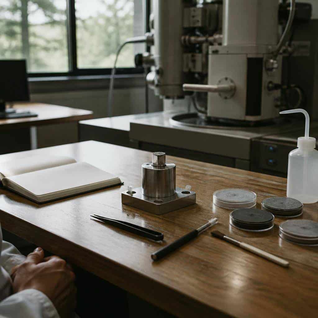
Achieving reliable and reproducible results in scanning electron microscopy analysis demands careful attention to the preparation steps, instrument calibration, and data interpretation protocols. This analytical technique, widely applied in material science and quality control, provides high-resolution surface imaging and elemental composition data, but precision depends on adherence to standardized procedures throughout the workflow.
Sample Preparation and Handling
The foundation of accurate microscopy analysis lies in meticulous sample preparation. Improper handling can introduce artifacts or degrade the surface morphology, which severely affects imaging quality and elemental detection. Best practices include:
- Cleaning the Sample Surface: Remove contaminants using appropriate solvents or plasma cleaning to prevent misleading signals.
- Mounting Techniques: Secure samples on conductive stubs to minimize charging effects; non-conductive materials require coating with thin conductive layers such as gold or carbon.
- Sectioning and Polishing: For cross-sectional analysis, ensure smooth cutting and polishing of specimens to reveal internal structures without inducing deformation.
Optimizing Instrument Parameters
Correct configuration of the electron microscope directly impacts resolution and analytical accuracy. Operators should carefully select accelerating voltage, working distance, and beam current based on the material properties and analysis goals. Specific considerations include:
- Accelerating Voltage: Lower voltages reduce sample damage and charging but may limit penetration depth; higher voltages improve resolution but risk beam-induced alterations.
- Working Distance: Shorter working distances enhance resolution but require precise focus adjustments.
- Detector Selection: Choose between secondary electron detectors for surface topology or backscattered electron detectors for compositional contrast.
System Calibration and Maintenance
Regular calibration ensures measurement accuracy over time. Key procedures involve aligning the electron beam, verifying magnification with standard reference materials, and calibrating energy dispersive X-ray spectroscopy (EDS) detectors for elemental analysis. Scheduled maintenance helps avoid drift, contamination, and hardware malfunctions that compromise data integrity.
Data Acquisition and Interpretation Strategies
Efficient data collection focuses on acquiring representative areas and minimizing noise. Operators should record multiple images at varying magnifications to capture both macro and microstructural features. When conducting elemental analysis, matrix effects and overlapping peaks must be corrected using software algorithms and reference standards. Cross-validation with complementary techniques strengthens confidence in results.
Common Challenges and How to Address Them
Users frequently encounter issues such as charging artifacts, contamination, and sample degradation during prolonged exposure. Mitigation techniques include:
- Using conductive coatings or low vacuum modes to reduce charging
- Applying minimal beam exposure time to prevent thermal damage
- Implementing rigorous cleaning protocols before analysis
| Parameter | Effect on Analysis | Recommended Range |
|---|---|---|
| Accelerating Voltage | Resolution vs. Sample Damage | 1-30 kV depending on sample |
| Working Distance | Focus and Depth of Field | 5-15 mm |
| Beam Current | Signal Intensity | Optimized per detector sensitivity |
Achieving reliable data in scanning electron microscopy hinges on applying these best practice principles consistently. From sample preparation to instrument calibration and data processing, each step influences the fidelity of analytical outcomes. Integrating these guidelines within routine laboratory procedures supports precise characterization essential for research, failure analysis, and quality assurance across diverse industries.